PCB Requirements for Typical SMT Equipment: A Scientific Overview
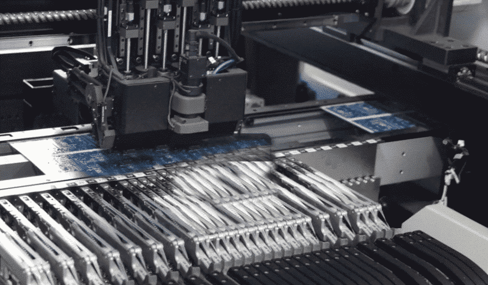
Printed Circuit Boards (PCBs) form the backbone of Surface Mount Technology (SMT) processes in electronics manufacturing. Proper PCB design is essential to ensuring the seamless operation of SMT equipment. This article presents a technical overview of the key design considerations required to meet the demands of modern SMT equipment.
Edge Considerations and Break-Away Tabs
Importance of Edge Design in PCB Manufacturing
SMT equipment, particularly conveyor-based systems, relies on precise rail transportation for positioning and assembly processes. To achieve this, the PCB must accommodate the rails effectively, often necessitating a 5 mm edge allowance along the transportation path. This ensures reliable fixation during soldering and component placement.
Break-away Tabs for Irregular Designs
For non-rectangular PCB designs, “break-away tabs” can be added to create parallel edges that align with the transport rails. Without these tabs, additional clamps or fixtures may be required to stabilize the PCB during the SMT process.
| Edge Design Parameter | Specification |
|---|---|
| Minimum edge allowance | 5 mm |
| Break-away tab thickness | 5 mm |
| Transport path width | Variable by machine |
Toaling Holes and PCB Positioning
Locating Holes for Precision in SMT Equipment
Positioning accuracy in SMT machines, such as screen printers and pick-and-place machines, is achieved using locating pins. This requires specific toaling (locating) holes in the PCB. Typically, two locating holes are positioned diagonally, one at each corner, to secure the board. The aperture of these holes is generally 4 mm, with their exact placement varying depending on the equipment used.
Optimal Placement of Toaling Holes
Toaling holes should be placed along the lower left and lower right corners of the PCB, ensuring that the holes are aligned with the machine’s positioning pins. When boards move from right to left through SMT machines, the hole at the left end should be 5 mm from both edges, while the right-side hole is positioned 5 mm from the bottom. To avoid interference, no components should be placed within 3 mm of the holes.
Baseline Requirements for Optical Positioning
Optical Baseline in SMT Systems
Most modern SMT systems rely on optical reference points for correcting PCB warping and positioning errors during the mounting process. These baselines consist of geometric shapes such as dots or circular holes, often with diameters of 0.8 mm or 1.5 mm. These points are distributed diagonally across the PCB to form a reference grid that ensures precise alignment during component placement.
Baseline Design for High Accuracy
Two baseline points are typically required for each PCB. The optimal placement is at diagonally opposite corners, ensuring that the virtual rectangle formed by their positioning encompasses all key SMT components.
| Baseline Parameter | Specification |
|---|---|
| Diameter of baseline | 0.8 mm or 1.5 mm |
| Clearance for dot (light point) | 1.5 mm around the dot |
| Clearance for hole (dark point) | 1.5 mm around the hole |
Tin Plating and Optical Recognition
Tin plating at the baseline points must create high contrast to ensure visibility under optical inspection systems. This contrast is crucial for automatic optical inspection (AOI) systems, allowing the equipment to accurately detect and position the PCB during production.
PCB Identification and Output Data
Data and Markings Required for Manufacturing
Once a PCB design is finalized, various identification markers and datasets must accompany the design into production. This includes labeling critical information such as the name of the PCB, component polarity, and production dates.
Documentation for Efficient Production
In addition to the PCB’s physical design, manufacturers require documentation such as the bill of materials (BOM), schematic diagrams, testing conditions, and quality control standards. For advanced testing needs, further documentation, including network tables and test conditions, must be provided.
| Required Data | Popis |
|---|---|
| PCB name and production date | Essential for traceability |
| Material list (BOM) | Specifies components required |
| Template and programming files | For manufacturing automation |
Conclusion
Standardizing PCB design for SMT equipment is critical for ensuring high-quality production processes. By adhering to design considerations such as edge allowances, toaling holes, and optical baselines, manufacturers can optimize the functionality and reliability of their products. This, in turn, enhances efficiency, reduces costs, and guarantees product quality—key drivers for any electronics manufacturer utilizing SMT technology.