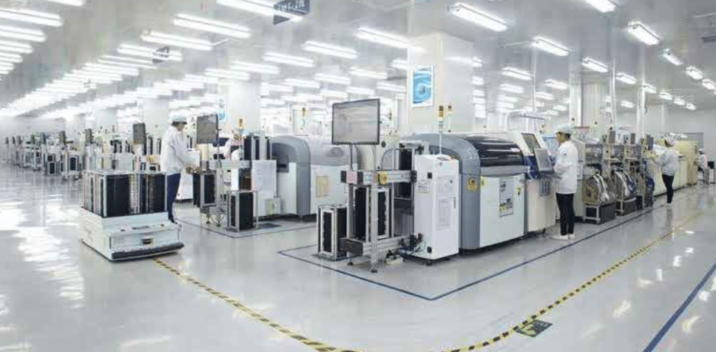
In the realm of PCB (Printed Circuit Board) design, optimizing cost without compromising quality is a critical aspect of the manufacturing process. To achieve this, careful consideration must be given to factors such as board size, component density, and technology choices. By adopting efficient methodologies, manufacturers can significantly reduce costs while maintaining the reliability and performance of the PCB.

Choosing the Right Technology: SMT vs. THT
One of the key decisions in cost-effective PCB design is selecting the appropriate technology. Surface Mount Technology (SMT) is generally more economical compared to Through-Hole Technology (THT). This is because SMT allows components to be placed closer together on the board, making the overall layout denser and more compact.
Component Density and Cost Implications
In SMT, the higher density of components reduces the size of the PCB, which in turn leads to lower material and manufacturing costs. However, this increased density requires more precise equipment and advanced materials to ensure that the wiring can handle power consumption and avoid circuit interference.
| テクノロジー | 利点 | Cost Implications |
|---|---|---|
| スマトラ | High component density, smaller PCB size | Reduces cost due to smaller boards |
| THT | Stronger mechanical connections | Higher cost due to larger board and complexity |
PCB Layer Count and Cost Considerations
The number of layers in a PCB directly affects its cost. While multi-layered PCBs provide greater functionality, they come at a higher price due to the additional materials and complexity involved in manufacturing. On the other hand, reducing the number of layers may lead to an increase in the overall board size, which could negate any cost savings.
Via Types: Buried vs. Through-Hole
The type of vias used on the PCB also plays a role in determining the final cost. Buried vias, which connect inner layers, are more expensive than traditional through-hole vias, as they require additional drilling steps during production.
| 経由タイプ | 料金 | Use Case |
|---|---|---|
| Through-Hole | 低コスト | Simple designs with fewer layers |
| 埋め込みビア | コストが高い | Complex, multi-layer PCBs |
Drilling and Hole Size Optimization
Another factor influencing the cost of PCB manufacturing is the hole size required for component pins. If the PCB design contains different types of components with varying pin sizes, the drilling process becomes more complicated. The machine must switch between different drill bits, which increases manufacturing time and, consequently, costs.
Standardizing Component Sizes
To minimize costs associated with drilling, it is advisable to standardize the pin sizes of components whenever possible. This reduces the number of different drills required, streamlining the manufacturing process and lowering overall expenses.
Testing Methodologies: Optical vs. Flying Probe
After the PCB is manufactured, testing is crucial to ensure functionality and prevent defects. Two common testing methods are optical testing and flying probe testing. While flying probe detection is highly accurate, it is generally more expensive than optical testing.
Choosing the Right Testing Approach
In most cases, optical testing is sufficient to identify any potential errors on the PCB, especially for simpler designs. Flying probe testing is reserved for more complex boards where precision is paramount.
| 試験方法 | 料金 | 正確さ |
|---|---|---|
| 光学テスト | 低コスト | Sufficient for simple designs |
| Flying Probe | コストが高い | Ideal for complex, high-density designs |
結論
Optimizing PCB design for cost savings requires a strategic approach that balances technology, layer count, via selection, and testing methods. By carefully considering component density, standardizing hole sizes, and selecting the appropriate testing strategy, manufacturers can significantly reduce the overall production cost without compromising on quality or performance. Through thoughtful design choices, it is possible to achieve an efficient, cost-effective PCB solution tailored to the specific needs of any project.
