


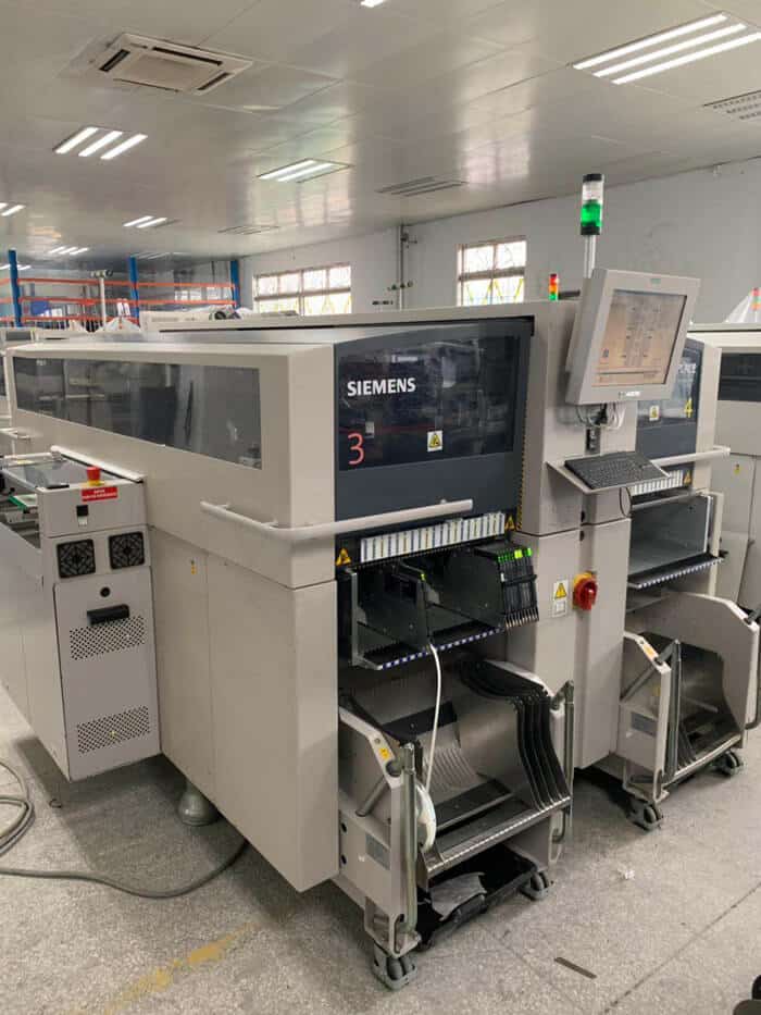

BUYSMT has been a game-changer for our electronics manufacturing. Your wide range of high-quality used SMT machines and components has allowed us to optimize our production line without breaking the bank. Your reliability and commitment to customer satisfaction are unmatched in the industry.

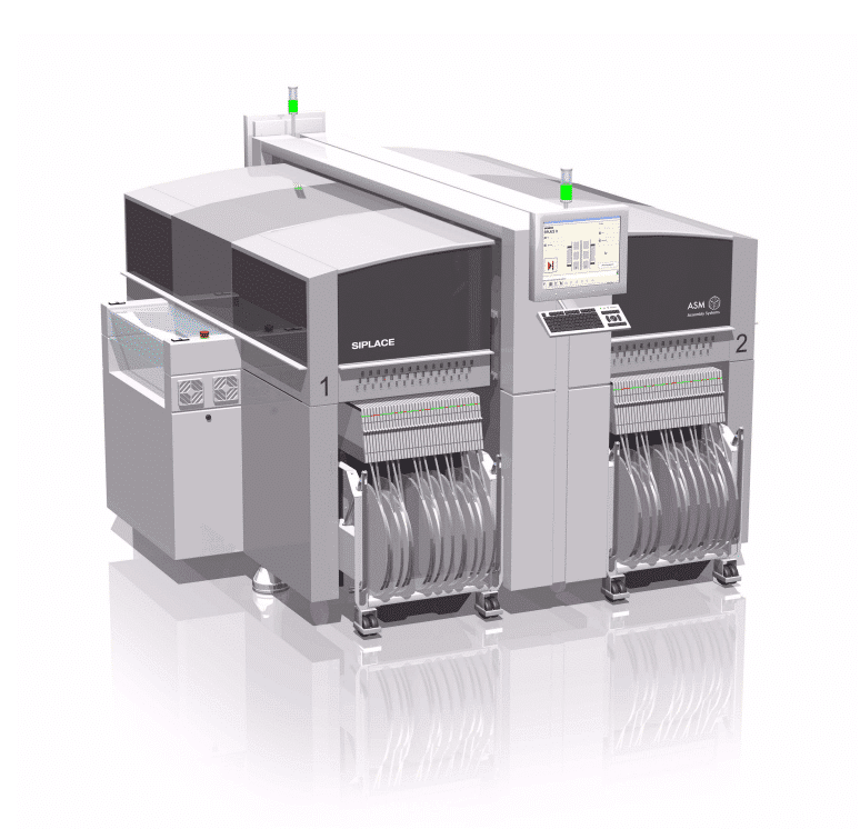
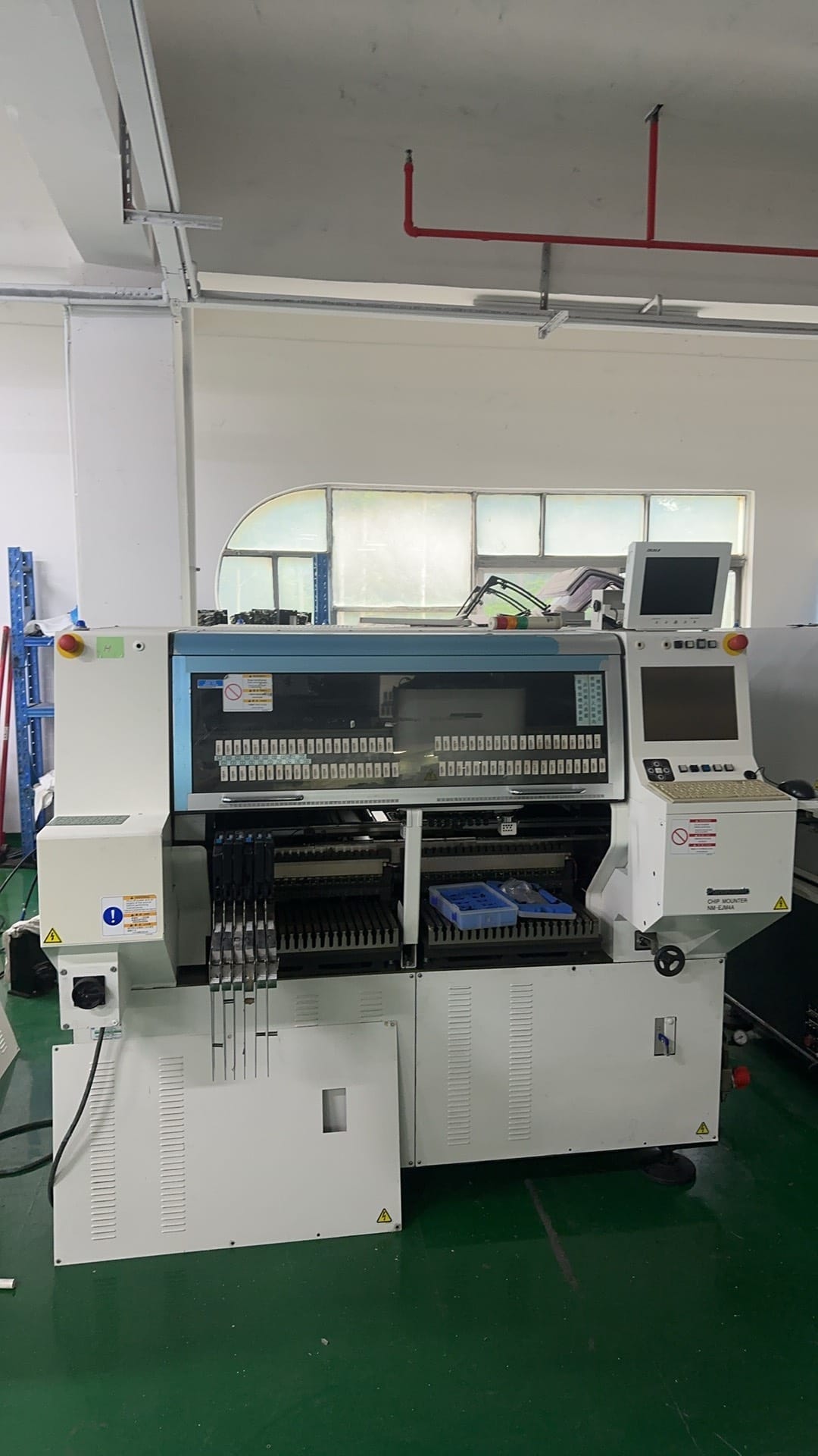
BUYSMT has provided us with the perfect solution for our budget-conscious project. Their used SMT equipment offers the same level of quality as new machines, at a fraction of the cost. We’ve been able to significantly reduce our production costs while maintaining high-quality standards.

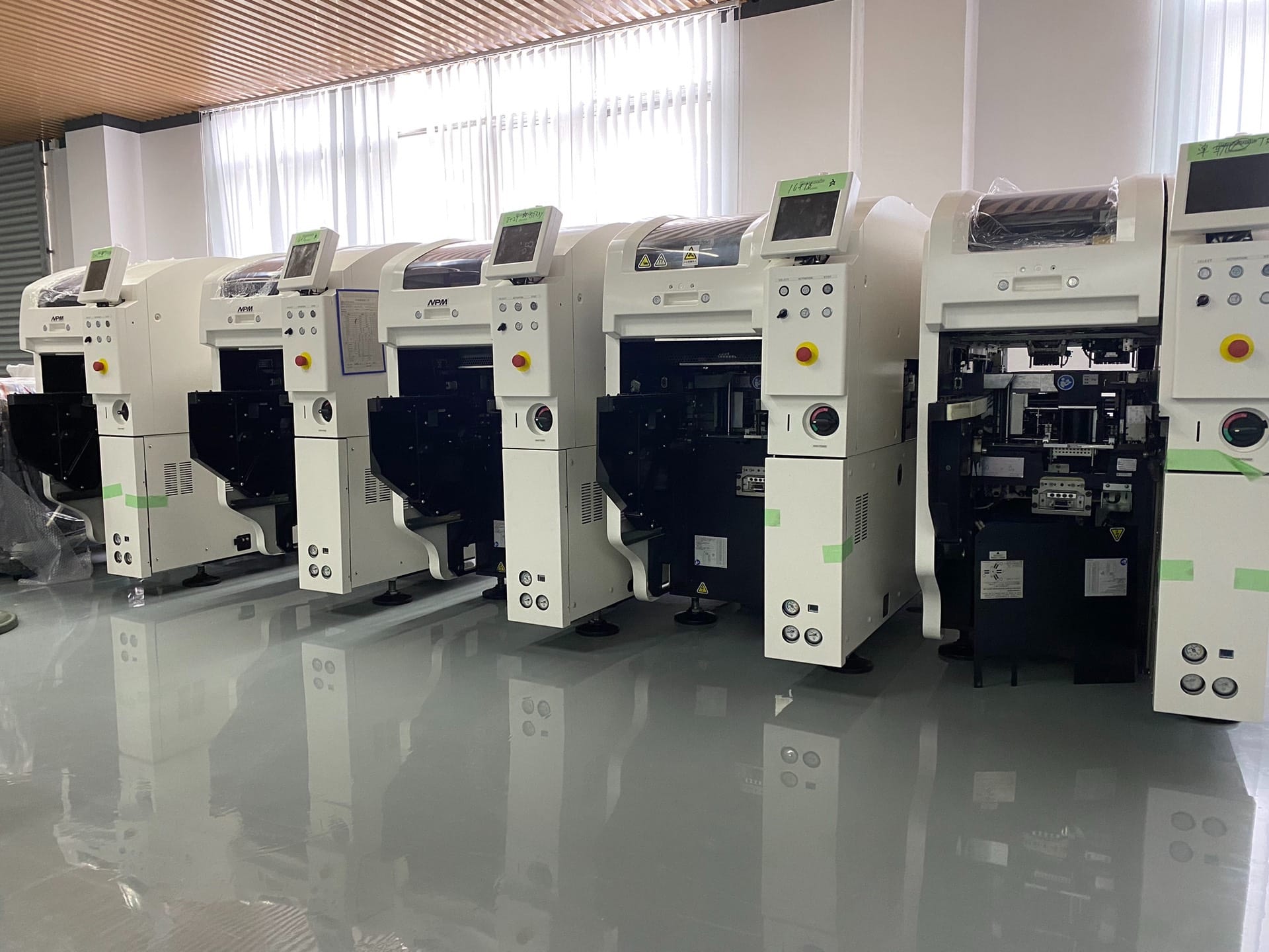
We’ve been working with BUYSMT for years and have always been impressed with their exceptional customer service. Their team is knowledgeable, responsive, and always goes the extra mile to ensure our needs are met. We highly recommend BUYSMT to anyone in the market for used SMT equipment.

We chose Buysmt because they offered a compelling economic advantage... and the trade-in process was straightforward and easy.